Hardware Overview rev. 2.8-rus
Версия от 19:07, 2 октября 2013; 46.39.244.90 (обсуждение) (Новая страница: «== Overview == This page describes Wiren Board rev. 2.8 (first public revision). The Wiren Board consists of two PCBs: * Olinuxino imx233-Micro with power capa…»)
Overview
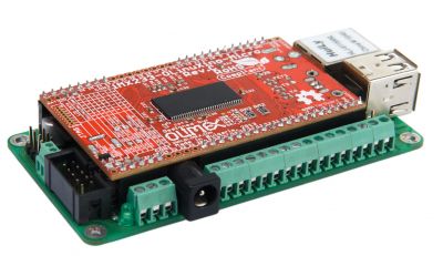
This page describes Wiren Board rev. 2.8 (first public revision).
The Wiren Board consists of two PCBs:
- Olinuxino imx233-Micro with power capacitors, TV out jack, power jack and USB jack desoldered. At present, original Olinuxino imx233-MICRO manufactured by Olimex is used. Most of the rev. 2.8 Wiren Board's are equiped with rev. C Olinuxino's. This board contains CPU (Freescale i.MX233) and RAM.
- Main Wiren Board PCB manufactured by Contactless Devices, LLC.
The main PCB contains:
- power management circuit based on LTC4002 chip.
- USB to Ethernet converter and USB hub, SMSC LAN9514
- USB Wi-Fi [[RTL8188_assembly|micro assembly] based on Realtek RTL8188 chip.
- NFC circuit based on NXP PN532. There is also trace antenna for NFC on the PCB. See also NFC Subsystem.
- Analog multiplexer for multiplexing 8 ADC channels (7 terminal blocks and Vin). See also ADC.
- SPI-to-UART bridge IC - NXP SC16IS752
- SPI GPIO expander - Microchip MCP23S08
- GSM/GPRS modem - SIMCOM SIM900R
Terminal blocks
| location | function | GPIO (if applicable) | olinuxino pin | comments |
| Terminal block 2 | FET/ADC | 32 | 3 @ CON1 | GPIO high to open FET; ADC channel 3 |
| Terminal block 3 | FET/ADC | 33 | 4 @ CON1 | GPIO high to open FET; ADC channel 0 |
| Terminal block 4 | FET/ADC | 34 | 5 @ CON1 | GPIO high to open FET; ADC channel 1 |
| Terminal block 5 | FET/ADC | 35 | 6 @ CON1 | GPIO high to open FET; ADC channel 2 |
| Terminal block 6 | FET/ADC | 39 | 10 @ CON1 | GPIO high to open FET; ADC channel 4 |
| Terminal block 7 | FET/ADC | 1 | 12 @ CON1 | GPIO high to open FET; ADC channel 6 |
| Terminal block 8 | GND | |||
| Terminal block 9 | GPIO/ADC | 2 | 13 @ CON1 | ADC channel 7 |
| Terminal block 10 | GPIO | 3 | 14 @ CON1 | |
| Terminal block 11 | GPIO | 4 | 15 @ CON1 | |
| Terminal block 12 | RS-485 A | UART1 from sc16is752, if RS-485 present | ||
| Terminal block 13 | RS-485 B | UART1 from sc16is752, if RS-485 present | ||
| Terminal block 14 | GND | |||
| Terminal block 15 | +3.3v | |||
| Terminal block 16 | +5.0v | |||
| Terminal block 17 | Vin | input voltage; ADC channel 5 | ||
| Terminal block 18 | GND | |||
| Terminal block 19 | Power FET | 60 | 28 @ CON2 | with PWM |
Externaly routed GPIOs
| 51 | 27 @ CON1 | UEXT2 I2C SCL |
| 53 | 28 @ CON1 | UEXT2 I2C SDA |
| 19 | 12 @ CON2 | UEXT1 CS/GPIO |
| 91 | 25 @ CON2 | UEXT2 CS/GPIO |
GPIOs for internal use
| 36 | 7 @ CON1 | ADC MUX A |
| 37 | 8 @ CON1 | ADC MUX B |
| 38 | 9 @ CON1 | ADC MUX C |
| 5 | 16 @ CON1 | IRQ |
| 6 | 17 @ CON1 | GPRS power key |
| 7 | 18 @ CON1 | GPRS reset |
| 16 | 19 @ CON1 | 3.3V rail shutdown |
| 17 | 20 @ CON1 | sc16is752 chip select |
| 50 | 25 @ CON1 | LTC4002 shutdown |
| 52 | 26 @ CON1 | MCP23S08 chip select |
| 92 | 24 @ CON2 | NFC PN532 chip select |
